TASKLED - Smart LED drivers
|
|
H6CC Buck LED driver Technical Information
H6cc Driver (New version 2024):
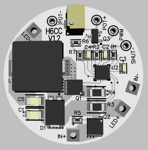
Version 1.2 driver board
Buck driver with SHUT- pin to shutdown driver to
low quiescent standby mode.
Magnetic Field Warning:
The H6CC is a switching regulator based driver and contains a shielded Inductor (L1 in the picture below). Strong external magnetic fields such as from a magnet used to operate a Hall sensor or Reed switch can interfere with the Inductor's operation. It is recommended to maintain a minimum of 1" from the Inductor and any external magnet. If the magnet is very powerful, then the distance needs to be increased (more than 1") as needed to minimise interference to the Inductor.
Potting Warning:
Areas of the circuitry on the H6CC driver utilises high impedance paths and if potting (only the top surface for water proofing etc) is to be utilised, the user must ensure than the compound is non-conductive and non-capacitive otherwise correct operation may be compromised. The same consideration is present if using thermal epoxy is used to mount the H6CC driver to a heatsink. H6CC ships with a piece of thermal pad material and it is recommended to use that material between the bottom of the PCB and the heatsink that the driver will be mounted to.
Hookup information:
The circuitry (all surface mount) fits neatly on a 1.20" diameter PCB on the top side. The maximum board+component thickness of the driver is 0.35" where the inductor (L1) is situated. Note, the thermal pad material is nominally 0.039" thick, so total thickness would be 0.35" + 0.039" = 0.389".
H6CC is capable of running from 8V up to 22V as shipped (guaranteed operating range). H6CC may operate as low as 5V, but operation between 5V and 8V is not guaranteed at the full 6.7A output current over the full operating temperature range (0C to 70C).
The picture shows the PCB layout. Only the top side of the PCB has components, the bottom side has a direct thermal interface to the components that require heatsinking. Provided with H6CC is a piece of thermal pad that is intended to be fitted between the bottom of the PCB and a heatsink. The mounting hole on the PCB is intended to be used to screw/clamp the PCB to the heatsink. The thermal pad material will conform to the heatsink and botttom of the PCB to provide an optimal thermal coupling.
The supplied thermal pad material is nominally 0.25mm thick, white in colour and will conform to the heatsink and PCB surfaces to provide an excellent thermal path. Please ensure the heatsink and bottom of the H6CC are cleaned of any grease or contaminants that would prevent the adhesive from properly bonding. Pressure should also be applied to help set the adhesive, refer to the datasheet for more information.
The thermal pad material (Li98 100 0.25mm) specifications can be found in the datasheet a copy of which is available here. The Li98 material provides a good compromise between the cost of the material and its thermal performance. The material is white in colour and has a protective cover on both sides that must be removed to expose the adhesive. Note, it is recommended to remove the Red protective material first and fix the pad to the heatsink or the H6CC prior to removing the white protective material. The adhesive is an acrylic base and takes up to 24 hours for fully cure/set. After a few thermal cycles and 24 - 48 hours the bond will become stronger and the thermal conductivity will improve.
Tests performed with 3 SST-50 equivalent LEDs driven at 6.7A via H6CC show that the H6CC PCB temperature will be at most 15C hotter than the heatsink when used with the provided thermal pad material. These results were with H6CC just resting against the thermal pad material (no pressure applied), so good performance without extra clamping force.
Connections:
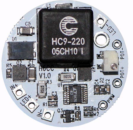
PCB (older V1.0 board)
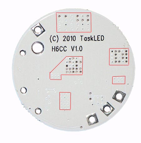
The next picture shows the back of the H6CC driver. The bottom of the H6CC provides a thermal path for the Inductor, Switcher IC, Reverse polarity FET and switching FET to the user provided heatsink. The mounting hole (0.136" nominal diameter) is provided to allow the board to be tightened down to the heatsink thus providing a good pressure contact between the board, the thermal pad material and the heatsink. The areas marked with the red polygons in the picture below are the key areas that need to make good contact with the heatsink via the provided thermal pad material. The small holes provide a thermal path through the PCB to the thermal pad areas of the IC's and the inductor.
Reverse polarity protection is implemented via a low Rdson FET (less than 30 mohms), so even at 6.7A input (worst case) the voltage drop would be only 6.7 x 0.03 = 0.2V.
Trimpot usage:
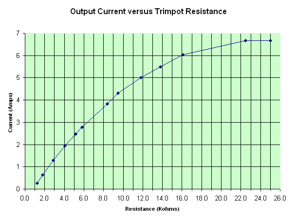
The trimpot (VR1) provides a way to adjust the current output of the driver. The minimum current output will go to zero (LEDs OFF). The maximum current that can adjusted is 6.7A (hardware limited by other parts of the driver circuitry).
The trimpot is in parallel with the external potentiometer, so it can be adjusted to compensate for deviation in the potentiometer resistance. Most potentiometers have a +/- 20% or worse specification for their open circuit resistance.
POT+ and POT- provide the connection point for an optional external potentiometer. To mimic the human eye logarithmic response to light intensity a 50kohm logarithimic taper potentiometer is a good choice. A linear taper will not appear to the human eye to have a linear response in intensity and is not recommended.
Note, the trimpot has a nominal life specification of 100 sweeps - so it should only be used to configure the current limit, not to perform the dimming function.
The following graph shows the current output versus resistance relationship. Measure the resistance from POT+ to POT- prior to applying power to the H6CC driver. Use a good quality multimeter.
SHUT- usage (H6CC V1.2):
This pin is optional and if left
unconnected, the driver will power up and function normally. If SHUT-
is driven low (<0.8V) the driver will enter standby mode and draw
minimal quiescent current. It is highly recommended to use an NPN open
collector transistor configuration to drive this pin low. When not
driven low, the SHUT- is pulled to the IN+ potential by a 100K
resistor, so ensure the transistor that is chosen can sustain IN+
potential on the collector-emitter specification.
PWM usage:
The PWM pin when driven above 1.5V will turn off the LED(s). Driving PWM below 0.4V will turn the LED(s) back on. Maximum PWM frequency is 500Hz with minimum 5% duty cycle. Maximum applied input voltage on the PWM pin is 10V. If the PWM feature is not required, leave it unconnected and the driver will function normally. The PWM will turn the driver on/off and it will drive the current set by the trimpot.
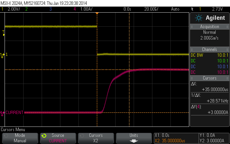
The following waveform shows the timing response of the LED output versus the PWM input signal. The top trace shows the PWM signal. The bottom trace shows the output current. As can be seen, the H6CC driver responds very quickly to the PWM signal. This test was performed with the H6CC set to a nominal 3A output. Cursors shows from PWM on (signal going low) to LED current reaching 3A takes around 35usec.
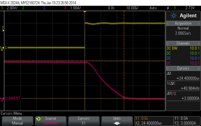
The following waveform shows the timing response of the LED output versus the PWM input signal. The top trace shows the PWM signal. The bottom trace shows the output current. This test was performed with the H6CC set to a nominal 3A output. Cursors shows from PWM off to LED current reaching 0A takes around 25usec.
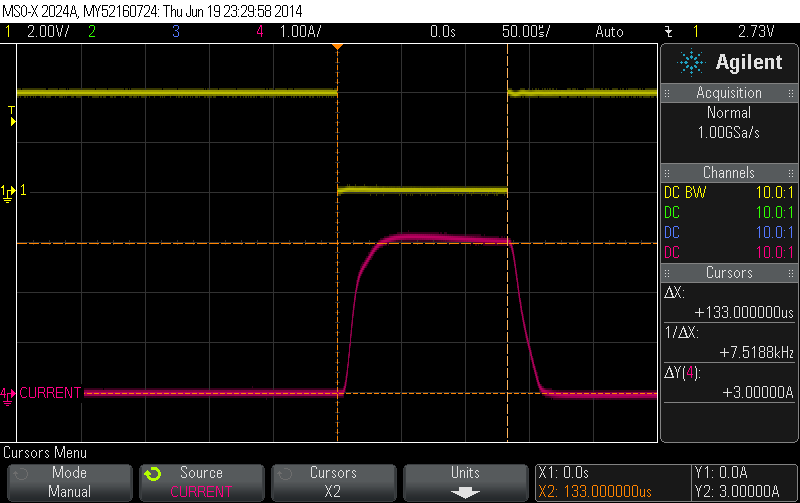
The following shows the response to a PWM pulse going off. 120uS on time is the shortest recommended pulse width to be used with the h6cc PWM input. Pulses shorter than 120uS will not provide sufficient time for the driver to fully regulate the output current.
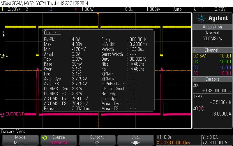
This screen capture shows the operating modes of the PWM signal for the tests performed above. On duty cycle is (100-96) 4% which is the minimum supported (5% minimum is recommended). The tests were run with 300Hz PWM frequency. 500Hz maximum is recommended.
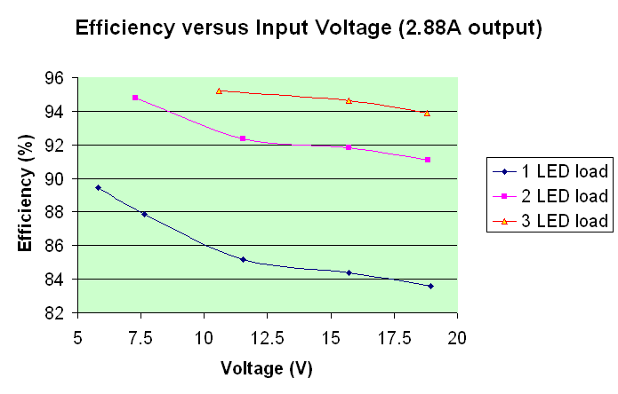
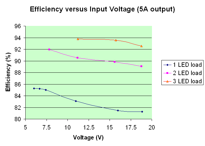
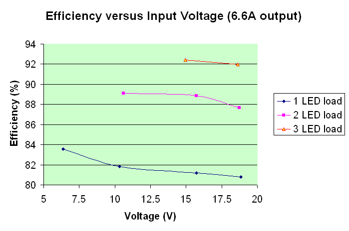
Efficiency of the H6CC is dependent on (input_voltage - output_voltage). The greater the difference between input voltage and output voltage, the lower the efficiency. Also, the driver is more efficient driving a higher output voltage than a lower voltage, i.e. 3 x SST-50 shows higher efficiency than 1 x SST-50.
Below are some efficiency curves illustrating the above points (1 LED approximately 3.5V Vf, 2 LEDs approximately 7V total Vf and 3 LEDs approximately 10.5V total Vf):
home | products | technical | order products | contact
©2026 TaskLED. All Rights Reserved.