TASKLED - Smart LED drivers
|
|
home > technical (HBFlex)
Operating Manual (PDF) for HBFlex:
Drivers shipped after Jan 20, 2014:
Drivers shipped prior to Jan 20, 2014:
Technical Information:
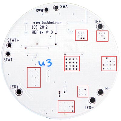
The picture below shows the bottom view of HBFlex. Marked areas on the bottom of the PCB are a direct thermal interface to the bottom of the power devices (on the component side of the PCB). If the power dissipation of the HBFlex board exceeds about 1W it is recommended to affix a heatsink or copper tab (to a heatsink) to the bottom of the HBFlex PCB using the supplied adhesive thermal pad material.
The supplied thermal pad material is nominally 0.25mm thick, white in colour and will conform to the heatsink and PCB surfaces to provide an excellent thermal path. Please ensure the heatsink and bottom of the HBFlex are cleaned of any grease or contaminants that would prevent the adhesive from properly bonding. Pressure should also be applied to help set the adhesive, refer to the datasheet for more information.
The thermal pad material (Li98 100 0.25mm) specifications can be found in the datasheet a copy of which is available here. The Li98 material provides a good compromise between the cost of the material and its thermal performance. The material is white in colour and has a protective cover on both sides that must be removed to expose the adhesive. Note, it is recommended to remove the Red protective material first and fix the pad to the heatsink or the HBFlex prior to removing the white protective material. The adhesive is an acrylic base and takes up to 24 hours for fully cure/set. After a few thermal cycles and 24 - 48 hours the bond will become stronger and the thermal conductivity will improve.
The X/Y position of the various solder pads/connection points is in the table below. X/Y position 0,0 is the center of the board. X/Y positions are in mils (0.001", so -75 means -0.075").
PAD |
X |
Y |
| STAT- | 605 | 75 |
| STAT+ | 590 | 175 |
| SWB | 160 | 595 |
| SWA | 45 | 620 |
| LED+ | 480 | -370 |
| IN+ | -465 | 400 |
| IN- | -465 | -370 |
| LED- | -370 | -465 |
Hookup information:
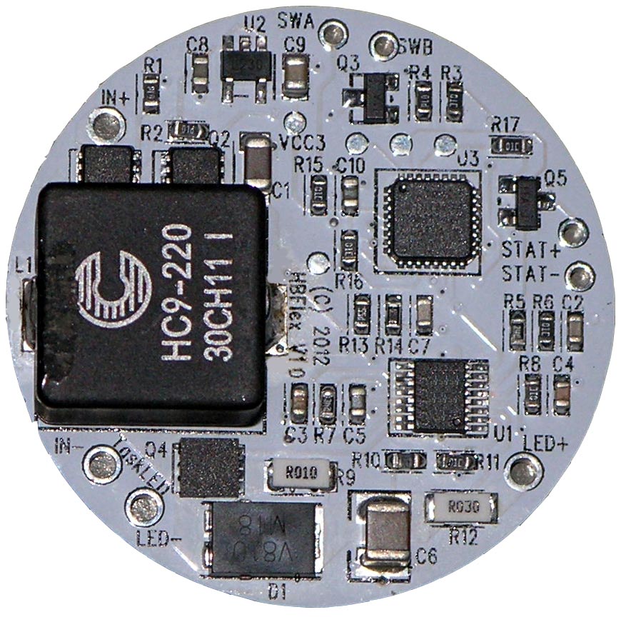
The circuitry (all surface mount) fits neatly on a 1.37" diameter PCB on the top side. The maximum board+component thickness of the driver is 0.35" where the inductor (L1) is situated. Note, the thermal pad material is nominally 0.039" thick, so total thickness would be 0.35" + 0.039" = 0.389".
The IN+ and IN- pads/holes are the input power connections to HBFlex. Pad hole diameter is nominally 0.055". 24V MAXIMUM input voltage (5 li-ion cells).
Input operating voltage range is 7V to 24V. HBFlex is capable (but not guaranteed) of running as low as 6.5V.
The LED+ and LED- pads/holes are the output power connections from HBFlex to the LED load. LED- IS electrically the same as IN-. Pad hole diameter is nominally 0.055".
The STAT+ pin can be wired the the cathode of a status LED. Pad hole diameter is nominally 0.040". The anode of the LED should be wired to a current limiting resistor and then to IN+. It is the user's responsibility to calculate the necessary resistor value to limit the current to the LED. The resistor value can be calculated using the following equation.
Resistor_value = (VIN - STAT_LED_Vf) / STAT_LED_CURRENT
As an example, for 10mA to a Red LED with Vf of 2.5V and running from 16V battery voltage:
Resistor_value = (16 - 2.5) / 0.010 = 1350 ohms.
STAT- is electrically the same as IN- and is typically not used.
The SWA hole is for one side of an external momentary action switch. The other side of the switch must be wired to SWB (which is electrically the same as IN-). The switch only switches a control signal and carries at most 350microamps. If using a magnetic reed switch, wire it across SWA and SWB. Pad hole diameter is nominally 0.040".
Note: it is recommended to keep the maximum wire length between the switch and HBFlex less than around 8 " (20cm). Having wire leads that are too long can cause the wires to act as an antenna and cause HBFlex to respond irregularly or turn on/off by itself.
The following picture shows the bottom side of the HBFlex driver. The areas marked within the red boxes are the areas that at a minimum need to be making contact via the supplied double sided adhesive thermal pad to a heatsink if the power dissipating of the driver exceeds 1W.
Note, HBFlex is a Boost regulator (step up), so input voltage must be less than the output voltage to ensure HBFlex remains in regulation. If the input voltage exceeds the output voltage (at the specified drive current), HBFlex will no longer regulate and the input voltage will go through the series inductor and schottky diode directly to the load. This will cause the output current to a LED to rise rapidly since LEDs have a very steep Current vs Voltage curve (Vf), with the risk of damaging the LED and/or the HBFlex driver.
The HBFlex user DC current regulation from 500mA to 3000mA (or whatever is configured as the maximum output current). Below 500mA the HBFlex transitions to PWM (running at 400Hz), so to determine the minimum LED Vf, 500mA can be used as the minimum drive current. HBFlex can drive as low at 50mA which is 1 in 10 duty cycle (1/10 of 500mA = 50mA).
Examples on how to calculate battery/LED combinations:
Step 1: Determine output power
Power_output = Number_of_LEDS * Vf * Output_current
Step 2: Determine input power
Power_input = Power_output/efficiency
For calculation purposes we can assume efficiency will be around 90% (or see the section below).
Step 3: Determine input current
Input_current = Power_input / Battery_voltage
Do this calculation for the lowest Battery_voltage you plan to run
Note, Input_current must be less than 7A for optimal performance of HBFlex.
Some Efficiency Measurements:
The HBFlex driver was connected to an Electronic Load and Powersupply utilising 4 wire sensing on both instruments to enable accurate efficiency measurements to be take.
Adequate heatsinking is essential when running at high output power.
The following table shows various operating points that were bench tested:
Vin (V) |
Iin (A) |
Vout (V) |
Iout (A) Nominal |
Pin (W) |
Pout (W) |
Calculated Efficiency |
| 7 | 1.5 | 10 | 1 |
10.96 | 10.03 | 91.5 |
| 7 | 2.4 | 15 | 1 |
16.79 | 15.11 | 90 |
| 7 | 3.25 | 20 | 1 |
22.63 | 20.16 | 89.1 |
| 7 | 5 | 30 | 1 |
35.19 | 30.59 | 86.9 |
| 7 | 7.2 | 40 | 1 |
50.6 | 41.52 | 82.1 |
| 11.1 | 1.48 | 15 | 1 |
16.56 | 15.33 | 92.6 |
| 11.1 | 1.97 | 20 | 1 |
21.89 | 20.38 | 93.1 |
| 11.1 | 3.01 | 30 | 1 |
33.46 | 30.94 | 92.5 |
| 11.1 | 4.13 | 40 | 1 |
45.9 | 41.98 | 91.5 |
| 14.4 | 1.52 | 20 | 1 |
21.9 | 20.4 | 93.2 |
| 14.4 | 2.31 | 30 | 1 |
33.23 | 30.98 | 93.2 |
| 14.4 | 3.13 | 40 | 1 |
45.1 | 41.87 | 92.8 |
| 18 | 1.21 | 20 | 1 |
21.7 | 20.47 | 94.3 |
| 18 | 1.83 | 30 | 1 |
32.92 | 31.04 | 94.3 |
| 18 | 2.47 | 40 | 1 |
44.52 | 41.87 | 94 |
| 7 | 3.1 | 10 | 2 |
21.8 | 19.5 | 89.4 |
| 7 | 4.7 | 15 | 2 |
33 | 28.7 | 87 |
| 11.1 | 2.89 | 15 | 2 |
32.1 | 29.76 | 92.7 |
| 11.1 | 3.9 | 20 | 2 |
43.25 | 39.73 | 91.9 |
| 11.1 | 5.96 | 30 | 2 |
66.13 | 59.72 | 90.3 |
| 14.4 | 2.968 | 20 | 2 |
42.75 | 39.87 | 93.3 |
| 14.4 | 4.53 | 30 | 2 |
65.24 | 60.34 | 92.5 |
| 14.4 | 6.186 | 40 | 2 |
89 | 81.3 | 91.3 |
| 18 | 2.37 | 20 | 2 |
42.62 | 40.2 | 94.3 |
| 18 | 3.56 | 30 | 2 |
64.18 | 60.39 | 94.1 |
| 18 | 4.82 | 40 | 2 |
86.84 | 81.18 | 93.5 |
| 7 | 4.87 | 10 | 3 |
34.04 | 29.46 | 86.5 |
| 7 | 7.6 | 15 | 3 |
53 | 42.9 | 80.9 |
| 11.1 | 4.44 | 15 | 3 |
49.24 | 44.88 | 91.1 |
| 11.1 | 5.96 | 20 | 3 |
66.2 | 59.68 | 90.2 |
| 14.4 | 4.5 | 20 | 3 |
64.79 | 59.88 | 92.4 |
| 14.4 | 6.9 | 30 | 3 |
99.36 | 90.29 | 90.9 |
| 18 | 3.57 | 20 | 3 |
64.32 | 60.3 | 93.8 |
| 18 | 5.4 | 30 | 3 |
97.2 | 90.53 | 93.1 |
| 18 | 6.58 | 36 | 3 |
118.44 | 109.08 | 92.1 |
To determine the heat being dissipated on the HBFlex driver, subtract the output power from the input power. Dissipating 10W from the hbflex is well within its capabilities as long as it is mounted with the supplied thermal adhesive pad material to an appropriate heatsink.
As power being dissipated increases beyond 1W the thermal path to the heatsink becomes critical to reliable operation. Most of the heat being dissipated in the driver is from the power FET Q4, D1 and the inductor, L1. The thermal interface (bottom of the PCB) is tied directly to the bottom of Q1, D1 and L1 using thermal vias. Additionally the input FETS (Q1, Q2) and the switcher IC (U1) have thermal vias to the bottom of the PCB. Mounting an adequate heatsink with the supplied thermal pad material is recommended and will allow HBFlex to be run at high power reliably.
Tests performed with 1 Bridgelux LED array driven at 3A with a Vf of 31V (total 93W output) via HBFlex show that the HBFlex PCB temperature will be at most 17C hotter than the heatsink when used with the provided thermal pad material. These results were with HBFlex just resting against the thermal pad material (no pressure applied), so good performance without extra clamping force.
Magnetic Field Warning:
The HBFlex is a switching regulator based driver and contains a shielded Inductor (L1 in the picture above). Strong external magnetic fields such as from a magnet used to operate a Hall sensor or Reed switch can interfere with the Inductor's operation. It is recommended to maintain a minimum of 1" from the Inductor and any external magnet. If the magnet is very powerful, then the distance needs to be increased (more than 1") as needed to minimise interference to the Inductor.
Potting Warning:
Areas of the circuitry on HBFlex utilise high impedance paths and if potting (not required) is to be utilised, the user must ensure than the compound is non-conductive and non-capacitive (e.g. Arctic Alumina - NOT Arctic Silver) otherwise correct operation may be compromised. The same consideration is present if using thermal epoxy is used to mount the HBFlex driver to a heatsink.
Rather than potting, it is recommended to use the thermal interface pad on HBFlex to connect to a heatsink using the supplied thermal pad material. NOTE, the thermal interface areas on HBFlex are NOT at ground potential.
home | products | technical | order products | contact
©2026 TaskLED. All Rights Reserved.