TASKLED - Smart LED drivers
|
|
Ultraboost Hookup Information: News Jan 2021 Ultraboost released.
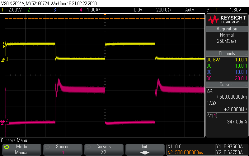
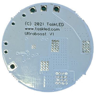
The picture below shows the production PCB.
The X/Y position of the various solder pads/connection points is in the table below. X/Y position 0,0 is the center of the board. X/Y positions are in mils (0.001", so -75 means -0.075")
|
PAD
|
X
|
Y
|
| IN+ | -125 | 555 |
| IN- | 60 | 560 |
| LED+ | 485 |
-305 |
| LED- | 220 |
530 |
| SHDN | 345 |
445 |
| POT+ | 590 | 20 |
| POT- | 585 | -100 |
| PWM | 495 |
315 |
| Mount Hole | 477 | 425 |
| Mount Hole | -516 | -381 |
The mounting hole x/y positions in the table above refer to the coordinates of the center of the 'Mounting hole'. Mounting holes are nominally 0.1" in diameter.
IN+ and IN-(GND) provide the power
input to the converter board.
Input voltage range is 8V to 50V.
Caution: Ultraboost can output up to 80V (no load or very long LED strings) and should be treated as a high voltage source that could shock the user in certain situations.
Note, Ultraboost is a Boost regulator (step up), so input voltage must be less than the output voltage to ensure Ultraboost remains in regulation. If the input voltage exceeds the output voltage (at the dialed in drive current), Ultraboost will no longer regulate and the input voltage will go through the series inductor and schottky diode directly to the load. This will cause the output current to a LED to rise rapidly since LEDs have a very steep Current vs Voltage curve (Vf). Ultraboost IS open circuit protect, it will limit output voltage to 80V (note this is high enough to potentially shock you if touched).
POT- and LED- and IN-
are NOT electrically identical.
LED+ and LED- provide the connection point to the LED(s).
POT+ and POT- provide the connection point for an optional external potentionmeter. To mimic the human eye logarithmic response to light intensity a 50kohm logarithimic taper potentionmeter is a good choice. A linear taper will not appear to the human eye to have a linear response in intensity and is not recommended.
PWM is the input to which a PWM signal can be applied to provide digital dimming.
SHDN is connected onboard to IN+ via a 100k ohm resistor. This will power the driver up by default. If the user wishes to power down the Ultraboost driver, the SHDN pin should be driven low (nominally 0V). In shutdown mode the Ultraboost draws less than 30uA. Maximum input voltage to SHDN is IN+ voltage.
Trimpot usage:The trimpot (VR1) provides a way to adjust the current output of the driver. The minimum current output will go to zero (LEDs OFF). The maximum current that can be efficiently provided to the LED(s) is dependent on the input voltage and the output voltage (total Vf of the LED load) and is hardware limited to a nominal 4000mA.
The trimpot is in parallel with the external potentiometer, so it can be adjusted to compensate for deviation in the potentiometer resistance. Most potentiometers have a +/- 20% or worse specification for their open circuit resistance.
Note, the trimpot (VR1) has a nominal life specification of 100 sweeps - so it should only be used to configure the current limit, not to perform the dimming function.
PWM usage:
The PWM pin when driven above 1.5V will turn off the LED(s). Driving PWM below 0.4V will turn the LED(s) back on. Maximum PWM frequency is 10kHz. Maximum applied input voltage on the PWM pin is 10V. If the PWM feature is not require, leave it disconnected and the driver will function normally. The PWM will turn the driver on/off and it will drive the current set by the trimpot.
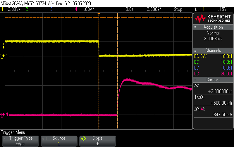
The limiting factor for the PWM control signal is the response time of the Ultraboost PWM circuitry and the LED driver IC. The scope capture below shows the current output response (nominal 2000mA output current) to the PWM input signal. The yellow trace shows the PWM signal being turned on (active low) and approximately 2us after the output current (pin trace) rising to at least 2000mA. The output current does droop a bit but settles back within 4us to the 2000mA constant current setting (set via the trimpot).
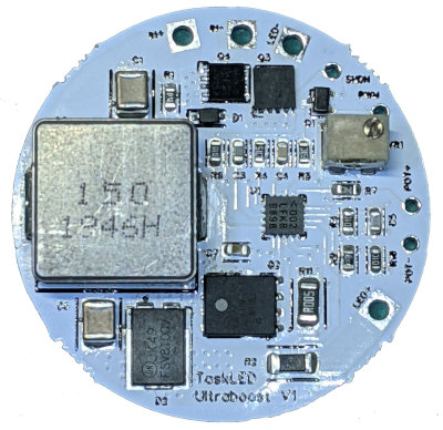
The next image shows the same waveform with the cursors showing the time it takes (less than 2us) for the LED current to decay to near 0mA after the PWM input is turned off (yellow trace goes back high).
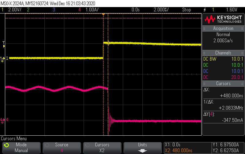
The following trace shows the same conditions as above, except that a couple of PWM cycles are shown. Each on/off cycle is about 500us.
Thermal/Heatsink considerations:
The next picture shows the key areas (the silver coloured polygons) on the bottom side of the Ultraboost PCB that require a good thermal path to the heatsink. At the minimum these locations require attaching to a heatsink via the supplied double sided thermal adhesive tape.
The supplied thermal pad material is nominally 0.25mm thick, white in colour and will conform to the heatsink and PCB surfaces to provide an excellent thermal path. Please ensure the heatsink and bottom of the Ultraboost are cleaned of any grease or contaminants that would prevent the adhesive from properly bonding. Pressure should also be applied to help set the adhesive, refer to the datasheet for more information.
The thermal pad material (Li98 100 0.25mm) specifications can be found in the datasheet a copy of which is available here. The Li98 material provides a good compromise between the cost of the material and its thermal performance. The material is white in colour and has a protective cover on both sides that must be removed to expose the adhesive. Note, it is recommended to remove the Red protective material first and fix the pad to the heatsink or the Ultraboost prior to removing the white protective material. The adhesive is an acrylic base and takes up to 24 hours for fully cure/set. After a few thermal cycles and 24 - 48 hours the bond will become stronger and the thermal conductivity will improve.
Magnetic Field Warning:
The Ultraboost is a switching regulator based driver and contains a shielded Inductor (L1 in the picture above). Strong external magnetic fields such as from a magnet used to operate a Hall sensor or Reed switch can interfere with the Inductor's operation. It is recommended to maintain a minimum of 1" from the Inductor and any external magnet. If the magnet is very powerful, then the distance needs to be increased (more than 1") as needed to minimise interference to the Inductor.Current setting table Ultraboost:
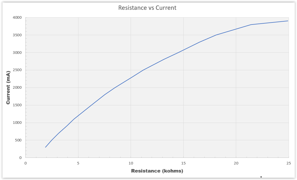
To adjust VR1 (the trimpot), measure the resistance with an ohm meter with probes across POT+ and POT- and then refer to the following table. Turning the trimpot clockwise increases the resistance and increases the output current.
|
LED Current |
Resistance
|
|
300 mA
|
1.9
|
|
500 mA
|
2.5
|
|
700 mA
|
3.2
|
|
900 mA
|
3.9
|
|
1100 mA
|
4.6
|
|
1500 mA
|
6.2
|
|
1800 mA
|
7.5
|
|
2000 mA
|
8.5
|
|
2300 mA
|
10.1
|
|
2500 mA
|
11.2
|
|
2800 mA
|
13.1
|
|
3000 mA
|
14.5
|
|
3300 mA
|
16.5
|
|
3500 mA
|
18.1
|
|
3800 mA
|
21.4
|
|
3900 mA
|
>24.9
|
Using the Ultraboost driver with an external Potentiometer to provide dimming control.
To connect an external Pot, one wire connects to the Wiper contact of the Pot to the POT+ on the PCB. A second wire from one end of the Pot connects to POT- on the PCB. The Pot should have a Logarithmic Taper (similar to Audio pots), this will allow the intensity to appear to change linearly to the human eye. The onboard trimpot is adjusted as per the table and graph above. Prior to adjusting the trimpot ensure the external Pot is adjusted to its maximum resistance. Then the procedure is the same as above, measure the resistance across POT+ and POT- and adjust the trimpot as above. A 50k ohm Pot is recommended.
Note: Ultraboost dims by lowering the output current. As the output current is lowered the Vf of the LEDs will also lower, so, it is possible that the output voltage (total of the LED Vf's) becomes lower than the battery input voltage. When this occurs no further dimming can occur because there is a DC path through the inductor and schottky diode (typical of boost converters) between the battery and the load and thus Ultraboost will essentially go direct drive.
Examples on how to calculate battery/LED combinations:
Step 1: Determine output power
Power_output = Number_of_LEDS * Vf * Output_current
Step 2: Determine input power
Power_input = Power_output/efficiency
For calculation purposes we can assume efficiency will be around 90%
Step 3: Determine input current
Input_current = Power_input / Battery_voltage
Do this calculation for the lowest Battery_voltage you plan to run
Input_current should be a maximum of 10A or less for optimal performance of Ultraboost. Beyond 11A the inductor specifications will be exceeded and efficiency will drop rapidly, do not exceed 10A as an absolute maximum. When running at high input power it is recommended to use the supplied thermal pad material to mount Ultraboost to a heatsink. Efficiency will drop as the output voltage/input voltage ratio increases.
Output Power::
Note, Ultraboost has been tested at up to 220W output. Beyond that power level the driver has not been tested or characterised.
The Ultraboost driver was connected to an Electronic Load and Powersupply utilising 4 wire sensing on both instruments to enable accurate efficiency measurements to be taken.
Adequate heatsinking is essential when running at high output power.
The following table shows various operating points that were bench tested:
|
VIN (V)
|
I (in) (A)
|
VOUT (V)
|
I (out) (A)
|
Power (in) (W)
|
Power (out) (W)
|
Efficiency
|
| 8 | 2.0 |
20 | 0.75 |
15.85 | 14.98 | 94.5 |
| 8 | 2.5 |
25 | 0.74 |
19.63 |
18.55 | 94.5 |
| 8 | 2.9 |
30 | 0.74 |
23.4 |
22.06 | 94.3 |
| 8 |
3.4 |
35 |
0.73 |
27.3 | 25.6 |
93.8 |
| 8 | 3.9 |
40 | 0.73 |
31.04 | 29.03 |
93.5
|
| 8 |
4.8 |
50 |
0.71 |
38.17 |
35.34 |
92.6 |
| 8 | 5.7 |
60 | 0.69 |
45.75 | 41.64 |
91.0 |
| 12 | 1.3 |
20 | 0.77 |
16.0 | 15.3 | 95.6 |
| 12 | 2.0 |
30 | 0.76 |
23.8 | 22.67 |
95.3 |
| 12 | 2.6 |
40 | 0.75 |
31.45 |
29.85 | 94.9 |
| 12 | 3.2 |
50 | 0.73 |
38.74 | 36.6 | 94.5 |
| 12 | 3.8 |
60 | 0.72 |
45.9 | 43.1 |
93.9 |
| 8 |
4.0 |
20 |
1.51 |
32.26 |
30.14 |
93.4 |
| 8 | 6.0 |
30 | 1.48 |
48.27 |
44.52 |
92.2
|
| 8 | 8.2 |
40 |
1.48 |
65.9 |
59.16 |
89.8
|
| 12 | 2.7 |
20 | 1.52 |
32.01 | 30.47 |
95.2 |
| 12 | 4.0 |
30 | 1.51 |
47.6 | 45.2 |
95.0 |
| 12 | 5.3 |
40 | 1.49 |
63.2 |
59.6 |
94.3 |
| 12 | 6.6 |
50 | 1.47 |
78.8 |
73.5 |
93.3 |
| 12 | 7.8 |
60 | 1.45 |
93.8 |
86.8 |
91.6 |
| 16 | 2.0 |
20 | 1.51 |
31.75 | 30.1 |
94.8 |
| 16 | 3.0 |
30 | 1.51 |
47.45 | 45.43 | 95.7 |
| 16 | 3.9 |
40 | 1.50 |
62.98 | 60.16 |
95.5 |
| 16 | 4.9 |
50 | 1.48 |
78.0 |
74.13 | 95.0 |
| 16 | 5.8 |
60 | 1.47 |
93.5 |
88.25 |
94.4 |
|
|
||||||
| 16 | 4.3 |
20 | 3.25 |
69.12 | 65.0 |
94.0
|
| 16 | 6.2 |
30 |
3.04 |
98.95 |
91.15 |
92.1
|
| 16 | 8.5 |
40 | 3.09 |
135.5 |
123.5 |
91.1 |
| 24 | 3.6 |
25 | 3.33 |
86.44 | 83.17 |
96.2 |
| 24 | 4.2 |
30 | 3.19 |
100.24 |
95.6 | 95.4 |
| 24 | 6.4 |
40 |
3.50 | 153.7 |
139.86 | 91.0 |
| 23.85 |
5.1 |
68.2 |
1.7 |
120.92 |
115.94 |
95.9 |
| 23.67 |
10.0 |
71.3 |
3.12 |
236.7 |
222.5 |
94.0 |
The second last entry is driving a Bridgelux
50G10X1C7 at rated output.
The last entry is driving the same Bridgelux at
way above its rated output, this was done for about 20 seconds and
stopped
before overheating/damaging the Bridgelux. Note that Ultraboost had
236.7W input and 222.5W output and was dissipating 14.7W of losses. The
heatsink and thermal path needs to be carefully selected to be able to
keep the Ultraboost operating within safe thermal limits.
home | products | technical | order products | contact
©2024 TaskLED. All Rights Reserved.