TASKLED - Smart LED drivers
|
|
home > technical (DualFlex)
Operating Manuals (PDF) for DualFlex V1.0/V2.0 hardware:
All Dualflex drivers ordered after March 21, 2015 ship with the UI-CAVE2 (Version 2) of the caving firmware. Please ensure you download the appropriate manual for the version of firmware that you have.
DualFlex 3D Step file: Click -> DualFlex.step to download.
UI-CAVE2 enhancements:
A short overview of the changes are listed below. Please refer to the updated manual for specific details. These changes are intended to offer more automated options on how the Main LEDs dim at specific voltage trip points and also how the battery voltage status is reported to the user.
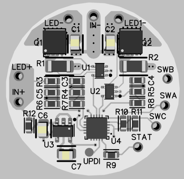
Technical Information:
LED1+ wired to anode of the
LED load (electrically the same as IN+), primary channel.
LED1- wired to the cathode of the LED load, primary channel.
LED+ wired to anode of the LED load (electrically the same as IN+),
secondary channel.
LED- wired to the cathode of the LED load, secondary channel.
IN+ wired to battery
positive.
IN- wired to battery negative. Do NOT wire battery negative to SWB or
you will compromise the current regulation path.
SWA wired to momentary action switch.
SWB wired to momentary action switch (electrically the same as IN-).
SWC wired to momentary action switch.
STAT wired to 3mm/5mm voltage status LED (max 2.5V drive with 100 ohm
series resistor on board).
Top side of the driver. This is the V2 Dualflex (released 2023), functionally the same as V1.
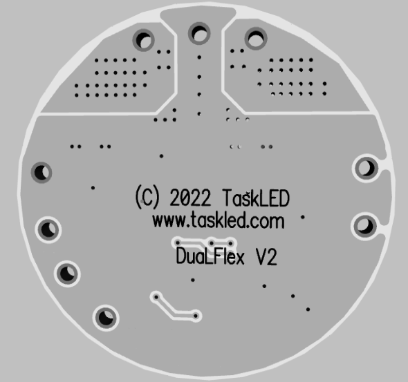
Bottom view of Dualflex V2.
The following block diagram shows how to connect the battery and LED(s) to the DualFlex driver. The diagram shows connecting a single momentary action switch (for UIC2W/C).
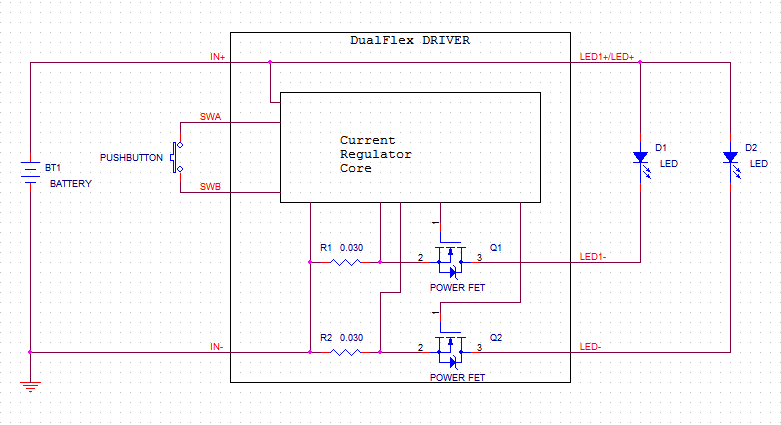
SWA/SWC and SWB (SWB is electrically the same as IN-) are provided to enable a momentary action (normally open) switch to be connected to DualFlex to control its operation. The switch only switches a control signal and carries at most 300 microamps. Even though SWB and IN- are electrically the same, SWB should be used only for the momentary action switch and IN- should only be used to connect to the negative of the battery.
Determining Power Dissipation:
The DualFlex driver is a linear regulated driver. It regulates the current by shunting excess voltage across the power FET. At higher currents, higher power is dissipated in the FET requiring the user to mount the PCB via the supplied thermal adhesive tape to the heatsink/body of the light.
The user should measure the Vf of each LED at the rated current. For example, if using two series XM-L LEDs, measure each Vf at the target current (say 3A) and sum the total Vf (lets assume they are 3.2, 3.3 for this example, so the total is 6.5V). Then take the fully charged battery voltage (say 2 li-ion cells) of 4.2 x 2 = 8.4V. Calculate the worst case power dissipation (difference between battery voltage and total Vf multiplied by the drive current). This power dissipation must be within the capability of the heatsink/body of the light to dissipate the heat.
First let's look at theoretical fresh off the charger li-ion cells that can output 4.2V even with a 3A load applied.
(8.4V - Total_Vf) x 3A = (8.4V - 6.5V) x 3A = 5.7 Watts. At this power dissipation level the FET requires substantial cooling efforts. In addition to mounting the bottom of the DualFlex to a heatsink with the supplied thermal pad material the user would need to provide a thermal path from the top of the FET package to a heatsink.
Next let's look at a real world 2 x 18650 fresh off the charger example with a 3A load applied.
At 3A current draw a li-ion cell (e.g. 18650) even freshly off the charger will drop to <4.0V within seconds of having the load applied. So, let's re-work the numbers assuming the li-ion cells drop to 3.9V per cell with a 3A load. (3.9 x 2 - Total Vf) x 3A = (7.8 - 6.5) x 3A = 3.9W which is well within the ability of the DualFlex to dissipate by mounting the bottom to a heatsink with the supplied thermal pad material.
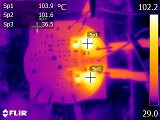
Thermal Imaging results:
The following images were taken with a thermal imaging camera with the DualFlex V3 board driving one XML LED per channel with a nominal Vf of 3.2V at 3A drive. The DualFlex driver is mounted to a substantial heatsink (block of Aluminium) with a piece of Bergquist BP100 thermal tape. FETs Q1/Q2 has an absolute maximum Junction Temperature rating of 150°C
FETs Q1/Q2 are the devices that will dissipate heat while the DualFlex driver regulates the output current. The two current sense resistors (R1 and R2) dissipate a constant amount of power for the selected output current. R1/R2 are 0.030 ohm resistors, so at 3A they are each dissipating I x I x R = 3A x 3A x 0.030 ohms = 0.27W. They are 1W rated resistors.
The first thermal image shows the driver running with 4.2V input and 3.2V (approximately) output @ 3A. This means the driver is dissipating (4.2V - 3.2V) x 3A = 3W per FET (6W total). FET Q1 reaches 103.9°C on the top surface (which will be close to junction temperature) as shown by point Sp1. The heatsink is nominally at 36.5°C (Sp2). FET Q2 is running a little cooler (101.6°C) since the measured Vf of the LED is slightly higher than the LED connected to Q1, this means slightly lower voltage drop and thus slightly lower power dissipation in Q2.
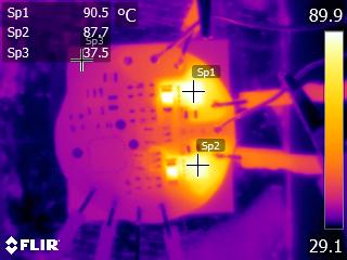
The next thermal image shows the driver running from 4.0V input and 3.2V output @ 3A. This means (4.0V - 3.2V) x 3A = 2.4W dissipation (per FET). FET Q1 reaches 90.5°C on the top surface and FET Q2 reaches 87.7°C.
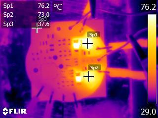
The next thermal image shows the driver running from 3.8V input and 3.2V output @ 3A. This means (3.8V - 3.2V) x 3A = 1.8W dissiption. FET Q1 reaches 76.2°C on the top surface and FET Q2 reaches 73.0°C.
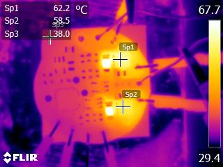
The final thermal image shows the driver running from 3.6V input and 3.2V output @ 3A. This means (3.6V - 3.2V) x 3A = 1.2W dissiption. FET Q1 reaches 62.2°C on the top surface and FET Q2 reaches 58.5°C.
Efficiency:
Some customers ask about the efficiency of the DualFlex. Well, being a linear regulated driver it works by dissipating excess voltage (x current) as heat. So, lets assume 4.2V in (one freshly charged li-ion cell) and 3.2V out (XML LED) at 3A (actually the current doesn't matter as will be seen in the calculation.
Efficiency = power_out/power_in x 100%
Efficiency = (3.2V x 3A) / (4.2V x 3A) x 100% = 3.2V / 4.2V x 100% = 76.2%
Now, let's assume the battery is somewhat discharged and at 3.7V.
Efficiency = (3.2V x 3A) / (3.7V x 3A) x 100% = 3.2V / 3.7V x 100% = 86.5%
Thermal Pad information:
The supplied thermal pad material is nominally 0.25mm thick, white in colour and will conform to the heatsink and PCB surfaces to provide an excellent thermal path. Please ensure the heatsink and bottom of the DualFlex are cleaned of any grease or contaminants that would prevent the adhesive from properly bonding. Pressure should also be applied to help set the adhesive, refer to the datasheet for more information.
The thermal pad material (Li98 100 0.25mm) specifications can be found in the datasheet a copy of which is available here. The Li98 material provides a good compromise between the cost of the material and its thermal performance. The material is white in colour and has a protective cover on both sides that must be removed to expose the adhesive. Note, it is recommended to remove the Red protective material first and fix the pad to the heatsink or the DualFlex prior to removing the white protective material. The adhesive is an acrylic base and takes up to 24 hours for fully cure/set. After a few thermal cycles and 24 - 48 hours the bond will become stronger and the thermal conductivity will improve.
Further information;
Battery input voltage can be from 2.7V to 12.6V (max), but power dissipation in the FET must be kept below 5W maximum if only the bottom side of the PCB is thermally mounted to a heatsink. Input voltage must be higher than the LED Vf at the selected drive current to ensure the DualFlex remains in current regulation.
Bottom side of driver:
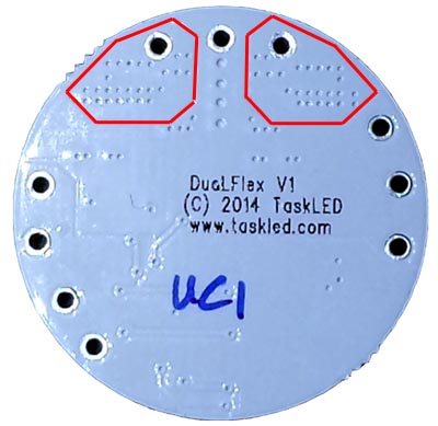
The red outlined areas in the picture above are the areas behind the power FETs that at a minimum must be thermally mounted to a heatsink or the body of the light. It is preferable to mount the entire board to a heatsink if possible.
home | products | technical | order products | contact
©2024 TaskLED. All Rights Reserved.